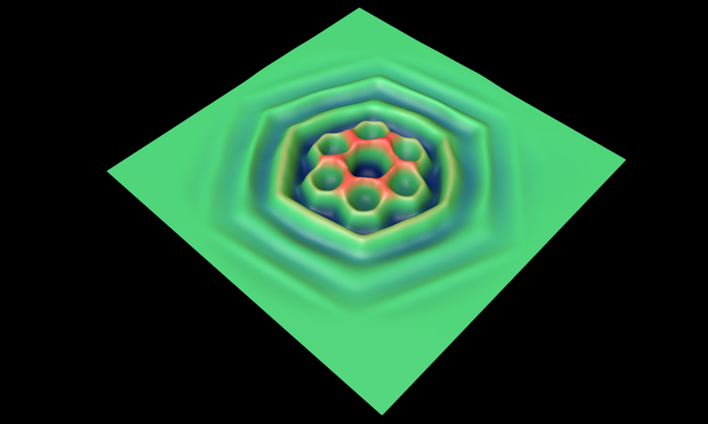
Artistic rendering of acoustic wave interference in lithium niobate domains measured by scanning microwave impedance microscope. Image credit: Ella Maru Studio
Thanks to a chance discovery, a team of researchers led by Keji Lai has developed a new imaging technique that could help researchers develop new materials and devices that use acoustic waves, such as communications devices, sensors or even cloaking materials to hide submarines from sonar.
The researchers describe their new imaging technique in this week’s edition of the Proceedings of the National Academy of Sciences.
Previously, Lai and his former postdoctoral advisor Zhi-Xun Shen at Stanford University developed a technique for studying the electrical properties of materials at the nanoscale called scanning microwave impedance microscopy (MIM). When Lai and his team applied this technique to a crystal called lithium niobate, they were surprised to see ripples in their images that shouldn’t be there.
“As physicists, when we see ripples, we immediately know that means interference,” said Lai, assistant professor of physics at the University of Texas at Austin. “Interference is a very unique feature for waves. If you drop two stones in a pond, you see the ripples on the surface and when the ripples meet, you see this interference pattern.”
After consulting with a colleague in the Cockrell School of Engineering, Zheng Wang, and running computer simulations, they concluded that the ripples were the result of acoustic waves.
“Our [microwave] probe is exciting the surface acoustic waves on the sample,” Lai said. “We’re putting in some electrical signals and we get mechanical motion.”
Essentially, they discovered a new way to image materials based on their acoustical properties. This could help speed the development of new sound-based materials and devices, as well as help manufacturers test the quality of their products.
It is currently possible to test materials for their acoustical properties with x-rays, but the process is complicated and expensive, requiring samples to be sent to a national laboratory. This new imaging technique can be done less expensively with modifications to atomic force microscopes that many university and industry labs already have.